Tuesday, 13 June 2017

Clock build log #3 - time decoders

This has to have been the easiest build of the project so far. I'm not quite sure why, but I was able to build this board from start to finish in about 3 evenings. It was certainly refreshing not having to spend weeks on it, and satisfying as the results were very rapid (rather unlike the timeliness of this post...)

The build starts as usual with the bus connectors. The time decoder board is going to be very much toward the front of the clock, in fact it'll likely interface directly with the display board, so it has all of the bus connectors on it, even if most of the pins within lay un-used by this board - it still has to carry all of the signals from the rest of the clock through to the display board.

I tried something a little different this time, however. In prior builds I had added supply (9V DC) and ground "busses" across the board as I went along, but it became a bit painful constantly modding new ones in as the build progressed, so this time I laid them all out in one go.


Then I start to solder in all of the transistors and resistors that will make up the gates. If you happen to be wondering how I get large numbers of them in at a time without a load of hassle, blu tack is your friend:


I borrowed the blu tack technique from Julian Ilett, a YouTuber that I follow (although I'm sure he wasn't the first to do it either, though he's certainly the first that I've seen do it...)

Then it's a process of wiring everything together on a decoder by decoder basis, and test each one as I go along so that I can catch faults progressively and early.

Testing was achieved with a "jig" that I rigged up on a breadboard. Although I had originally planned to, and thought that I had bought common cathode displays, it turns out I bought common anode displays instead. Using common cathode I had planned to have the final "driving" gates of the decoders control the flow of current to the LED segments, but now with common anode displays I'll be sticking resistors and transistors on the display board along side the displays they will control. The transistors will connect the cathode of each segment down to ground when its decoder output is high, so it'll achieve the same result but use a few more transistors and resistors (not like I'm short of them...)


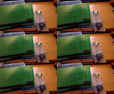
In the right hand picture above you see what is the units seconds decoder connected to the time module and then onwards to the test jig. I even managed to create an animated GIF showing it counting through all of the digits.

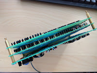
I worked my way through all 6 of the decoders very quickly and they all worked without a hitch so unfortunately there's no troubleshooting to speak of, but here's the end product including a bonus photo of how the stack is coming along now (and it's starting to feel kind of weighty!):


On to the next one I guess!

Wednesday, 31 May 2017

Clock design log #3 - time decoders

With the time module built and tested, I need a way to display that time in a more human friendly format, or at least the intermediary step towards that. Interfacing between the binary coded decimal (BCD) values that the time module puts out and the 7 segment displays requires a series of decoders that I covered in one of my very first posts, since what the time module outputs is not directly useable to drive a display - unless I wanted to build a clock that reads in binary.

This is where all of the earlier work with k-maps comes in to play. The decoders are not much more than combinational logic, taking the binary values as inputs, and turning the right outputs on to light up individual segments to produce the required display. There are no counters or SR latches or reset circuits as the decoders are completely stateless.

The time decoder board will have 6 decoders on it, one for each 7 segment display required to show the time in 24 hour format: HH MM SS

One of these decoders, the tens decoder for the hours (left hand most display) is a 2 bit decoder since it only needs to display values 0, 1 and 2. It will still decode a value of 3, because I'll re-use the same design in the day of month decoder when it comes time to build the decoders for the calendar module, but the time module never outputs a value of 3, so that should never appear on the display.

The tens decoders for minutes and seconds are both 3 bit decoders able to show values from 0 to 5, permitting the display of numbers up in to the 50's.

And the units decoders for hours, minutes and seconds are all 4 bit decoders which can show values from 0 to 9.

Put them all together and that gives the decoders the ability to display any combination of hours, minutes and seconds from 00:00:00 through to 23:59:59.

Rev B decoders

During the course of posting on my blog I've been conversing with one particular person on a reasonably regular basis, I believe his name is Matthias. In response to my post about designing 7 segment decoders he posted that he was able to reduce the gate/transistor count of some of them by not decoding digits 6 and 7 for the 3 bit counter. I'd kind of deliberately not bothered to do that, but it did get me thinking that perhaps I should. And having built the time module and realising how complicated and time consuming the construction process can be, reducing the number of gates and transistors is probably a good thing for my sanity. So I decided to use a re-designed version of the 2 and 3 bit decoders to reduce their part count. I was quite happy with the 4 bit decoder design so I havent touched that.

The new k-maps I came up with are available in this spreadsheet, and at the end of the post you'll find a link to revised logicly files and images which I used to verify their operation. These are the final designs I used to build my decoders.

I could have likely made them even more compact if I made them more (what I call) "loose", i.e. some values would match, and would produce some strange looking output on the 7 segment display, but you're not likely to encounter those values due to the preceeding logic in the clock. This can help to simplify some of the minterms, which requires fewer components to implement. But I decided not to do that, opting to strictly decode only the values that I want, and out of range inputs will result in a blank display.

The result of the revision of these two decoders is a reduction in transistor/gate count per the following:

  • 2 bit decoder: originally 18 transistors and 14 gates, now 13 transistors and 10 gates
  • 3 bit decoder: originally 56 transistors and 26 gates, now 35 transistors and 22 gates

Quite a large saving on the 3 bit decoder.

The good stuff

So here are the design files for the time decoders. Usual formats include EAGLE schematic files and a PDF export, plus the logicly designs for the revised decoders.

Wednesday, 24 May 2017

Clock build log #2 - time module

Build

Build for the time module started with the bus connectors that would connect to the analogue board and further in to the stack. The connector for the analogue board is a small 8 way pin header, while the connector for the rest of the stack is a 40 pin socket - but not one with extended pins. Positioning of this board within the stack is somewhat limited, as it connects to the analogue board and in doing so it bridges power and the MCLR, AC_CLK/ and 1PPS_CLK/ signals through to the larger bus. That means this board pretty much has to sit adjacent to the analogue board for the bus connectors to line up properly between the two. It all started off looking so simple:


Then I started what would become a (part time) month and a half long process of soldering in transistors, resistors and jumper wires to create the gates that would form the logic.

While putting the seconds counters together I had an idea - what if I was to use the 1PPM clock signal that it creates to collect some statistics about how much the AC frequency drifts? I thought it would be kind of interesting to see just how wild the AC frequency was, and how often and for how long it drifts around. As part of this I thought it would give a nice insight in to how quickly things might degrade and how long it takes to recover.

So after soldering in the first 56 gates worth of transistors that make up the seconds counters and their reset logic (which generates the 1PPM_CLK/ signal) I branched off in to a small software project.

I had a Raspberry Pi sitting idle that I thought would be perfect for the task, since it has GPIO pins that I could interface to my clock. I knocked together a small program in C that, upon start, takes the current UNIX timestamp when the first 1PPM clock pulse occurrs, and for every subsequent 1PPM clock pulse it records the UNIX timestamp again, substracts the difference, and outputs the timestamp and difference. I piped that information in to a file and then left it to run for about 2 weeks until something started going funny and it started missing pulses and producing erroneous results.

I tried applying some manual fixes to some of the data, and restarted the script a couple of times before it started getting too out of hand and I gave up, sticking with about 11 days worth of solid data, or about 15,700 records. From that I was able to produce the following graph by loading all of the data in to a spreadsheet:


Since I don't know when "zero" is for the AC mains frequency, "zero" for me and my exercise was at UNIX timestamp of 1491865936, which for the non-techies means April 10th 2017 at 23:12:16 UTC (basically it's the number of seconds since January 1st 1970 00:00:00).

This answered two questions:
  1. How much the clock may end up drifting - over my sample of data as much as +22 and -35 seconds
  2. How quickly or slowly it drifts and recovers - could be as quick as a single day to a couple of days
Re #2, April 17th was a "bad day" where it slowed right down to the slowest it ever got, while we see that over the 13th and 14th we caught up 20 seconds and went 10 seconds faster still.

The most important thing I learned from this was that the clock would probably eventually come back to zero offset. So some of my worries about how reliable the AC frequency was going to be ended up being addressed through that little exercise. At least it wasnt going to be constantly getting slower and slower or faster and faster and never return, though long term results are yet to be seen...

Here are a couple of photos/images showing the setup I used to collect the data for the above graph, and also the schematic for what's happening on the breadboard (a MOSFET level translator, since the Raspberry Pi GPIOs are 3.3V and my clock is 9V):


Funnily enough, this is the first time I have ever used a Raspberry Pi for the thing that I guess it was intended to be used for - tinkering with electronics. My other Raspberry Pi's are running FreeBSD or Linux and acting as servers more or less. :-)

Back to the task at hand... it pretty much just sounds like a broken record from here. Solder, test, repeat. So theres not really much more to say about the build. And it seems I didn't take many more photos during the construction process, so theres a distinct lack of more things to say or show right now. So perhaps the more interesting and juicy bits are in the testing of what I have built.

Testing

Learning from the build of the analogue board, I built each counter stage individually and tested that it worked as expected before moving on to building the next. This meant that solder joints weren't buried under so many wires and hard to get at. It also gave confidence that as I was going along and things were working, if anything happened to stop working further on during the build it might likely be what I was just working on rather than something earlier on. At least then it would be a process of test the most recently built circuit and then start moving backwards if that was checking out OK.

With the seconds counters working just fine, the first major problem I came across was with the minutes counter. When I started building it one of the first things I did was to hook up the button with its debounce circuit so that I could advance that counter manually, instead of having to wait for the 1PPM_CLK/ signal to fire, although testing that the counter advanced on that clock pulse was also important.

Advancing of the units counter was fine, but I noticed an issue when it came to the reset event. The counter would advance, and at 10 count the output of the gate hooked up to the outputs of the 2nd and 4th stages would go high, inverting an SR latch to reset the counter back to 0. But after doing that, the SR latch wouldn't release that reset, so the counter could no longer advance (well, it would have if I had actually hooked up the reset inputs of the counter stages, but I hadn't at that point in time). I traced out all of the wiring I had soldered and realised the issue was not with the design or build of the time module circuitry, but with how the AC_CLK/ signal was handled back on the analogue board.

On the analogue board is a switch that allows you to isolate AC_CLK/ from the clock to stop it advancing the mains frequency prescaler, thus allowing you to reset the clock to all zeros and then set it manually without it carrying on, then set it running once you were ready. But that switch isolated the AC_CLK/ signal from the entire clock, and while it did what I had originally intended it to do, it was breaking another piece of functionality - when an SR latch it set by a connected "AND" gate to cause a reset, it needs the AC_CLK/ signal to release that reset! Ooops. So a quick re-design of the AC_CLK/ circuitry such that the switch only isolates AC_CLK/ from the input of the first counter stage mains frequency prescaler was in order, and luckily that was pretty simple, and required minimal re-work. The revised schematic will be linked below.

Here are some scope traces that show the incorrect (left) vs correct (right) behaviour:


Some explanation of what you're seeing ... the yellow trace is the inverted output of the SR latch on the minutes units counter (i.e. the one that would generate the 1PPH_CLK/ signal in this case). That output clocks the input to the minutes tens counter, hence it has gone from high to low in the left hand image. But you see that, while D4 has gone high (being the first stage of the minutes tens counter), D1 and D3 have not gone low, and the yellow trace remained low.

At the time I took that trace, the switch isolating the AC_CLK/ signal from the clock was set to the "stop" position. If I had set that to "run" things would reset correctly. But it's a bit silly to need the clock to be in "run" mode for this to work correctly, its kind of the complete opposite of what I was aiming for.

After modifying the circuitry around that switch, I took a second capture which is the right hand image you see above. As you can see things are a bit different here. As D1 goes high towards the right hand side of the trace, it remains high only for a very brief period of time, hence you just see a "glitch" in the trace for that signal. When it does go high, and with D1 and D3 representing 2+8, that generates the reset condition for that counter, so D4 goes high. You also see a very brief glitch in the yellow trace - thats the SR latch being set by the "AND" gate of the minutes unit counter and then being reset by the AC_CLK/ signal, and all with the switch being set to "stop". So that was now sorted and working correctly.

For interest sake, here's an even closer look at whats happening when the reset of the minutes unit counter occurrs, which pretty well matches the description that I gave in design notes #5 - it's nice to know that my theory turned in to reality 😎 :


At the bottom you see that I have grouped the digital channels in to some busses, B0 (D0-D3) and B1 (D4-D6), and they are displaying what you'd see on the display if the decoders were built. As we lead in from the left, we're at 09, and at the next button press D0 goes low (and for a very brief period of time we go backwards to 08) until D1 goes high and we get to a value of "A" in base 16 (aka hexadecimal) which equals 10 in our every day base 10/decimal system. At that point the reset condition is created and after 20 odd uS D1 and D3 go low while D4 goes high, and now we see that the value on the display would be 10.

Fortunately there were no more surprises that needed fixing in the build from here on, and things went smoothly. All counters worked as expected, and all clock pulses were generated fine and dandy. Somewhat boring, but also somewhat relieveing since ...

End result

... heres what I ended up with!


That was quite a bit of work!

But most importantly it works, much much much to my relief. Along with producing the 1PPD_CLK/ signal when rolling over from 23:59:59 to 00:00:00, it also produces 1PPM_CLK/ and 1PPH_CLK/ signals, although at the moment there is nothing planned that uses these, except perhaps 1PPH_CLK/ which might be used by another module to do display dimming/blanking.

Luckily I think this will be one of, if not the busiest board in the clock - it's certainly going to be one of the most densely populated. I anticipate that the calendar decoder board might be pretty complex/dense too, but we'll have to wait and see what that one brings (designs still pending at this stage...)

In closing, along with the revised analogue board schematic, I've uploaded the C source for the program I wrote to capture data for the graph, and I have also uploaded an updated schematic for the analogue board with the fix for the AC_CLK/ generator. C is not my every day programming language, so please be gentle (and you'll need wiringPi to make it work).

Thursday, 18 May 2017

Clock design log #2 - time module

The next board in the stack will be what I call the "time module". I call it this because it uses the 1PPS_CLK/ signal from the analogue board as its input, and using that it keeps track of the time time - and thats all it does. At what would be 24:00:00 it resets to 00:00:00 and generates the 1PPD_CLK/ signal which is used by what will probably be known as the "calendar module".

If you haven't already read my post about operating theory, it would be worth it before going much further with this post, it should help you understand whats going on in the schematics better. I'll re-cover a little bit of the theory here, but not in too much detail.

The basic premise of the time module is to implement 6 ripple counters, each of which has its own reset circuit that resets the counter at the appropriate value and clocks the next counter, and whos BCD values will be fed in to a set of decoders, each of which will drive a particular display at the front of the clock.

If you recall back to an earlier post, I mentioned that I had really wanted to implement these as 3 larger counters, but the decoders to drive the displays were getting very complicated, so I had to settle for 6 smaller counters. The idea behind this is that each portion of the display (that is, seconds, minutes, and hours) contains a "units" counter and a "tens" counter. A units counter will count 0-9 while a tens counter will count 0-5 (or 0-2 for hours). As each counter resets it clocks the next counter, so when the seconds unit counter "rolls over" from 9-0 it will clock the tens counter which will increment by 1. When the seconds tens counter "rolls over" from 5-0 it clocks the units counter for minutes, and so on and so forth. I guess its similar to how odometers in older cars work in a way.

As you're looking through the schematics for the time module, you'll see a lot of repeated circuitry which are D type flip flops that make up the individual stages of the ripple counters, and you will also see some other regular circuitry to the left of the ripple counters which is the reset logic for that counter. Above each counter will be a NOR gate facing in the opposite direction to all of the others, and this acts as an "AND" gate which feeds in to an SR latch. When the inputs to the "AND" gate are at appropriate values (in this case, all low because it uses inverted logic being a NOR gate) its output goes high and inverts the SR latch. When the SR latch inverts it causes the ripple counter to reset to 0 and generates a clock pulse to the next counter. The AC_CLK/ signal then inverts the SR latch again a short while later, and the counter can then start counting from 0 again.

Other gates just ensure that, for example, when MCLR is asserted (e.g. by pressing the reset button), if the input to the first stage of each counter was high it will actually be able to reset, and some other multiplexing such that either the SR latch or the MCLR signal is able to reset the counter. You will also notice that the minutes and hours units counters also include an input which allows those counters to be incremented manually by pressing a button. This is so that a value can be loaded in to those counters in order to set the time (e.g. after power on or user reset).

The hours counters are really the only "tricky" exception. Seconds and minutes reset at a decade boundary, but hours counts to 24 before resetting. So while there are still two gates which feed in to SR latches to initiate the reset, you'll notice that one of them actually causes not only the tens counter to reset but also the units counter, and in order to do that it takes input from the units and tens counters - that's unlike any of the others, which only take their inputs from the counter they are resetting.

And with that, the only thing left to do is to link you to the schematics:
Enjoy!

Friday, 12 May 2017

Clock build log #1 - analogue board

Alright, alright already! I know this is what some people have been waiting for - actual freakin' construction. So I'll just get straight to it.

Build

I started with construction of the power supply, since that was going to be rather necessary. For a slight retro look I decided to use an axial capacitor as the smoothing capacitor on the input to the linear regulator. The full bridge rectifier has a 100nF capacitor in between the DC terminals as I read this can be good for filtering noise at the output of the rectifier. This then feeds via the smoothing cap in to the 7809 regulator. Another 100nF cap at the output of the regulator helps to filter noise on the output here too (not that I expect that much noise, but it can't hurt) and the positive rail then feeds through a PTC (fuse) for short circuit protection - theres a lot of fiddly wiring all done by hand, and if I happen to short something out or it breaks loose, I don't want anything getting damaged.

It was hard to find a 2.1mm DC jack that wouldn't need me to drill in to my board to create slots that the terminals could be inserted in to for soldering (i.e. nothing with pins on a 0.1" grid), but I had a flash of inspiration and figured that a surface mount jack with some loops of wire over the top of its terminals could be used to make my own "through hole" socket, so thats what I did, and this is what I ended up with for the power supply:


Quite pleased with that result, and the DC jack feels very solid. I used the off cuts of the rectifier diode leads to form the loops as they were quite hefty.

Next came a sprinkling of other building blocks and bits and pieces: the power on reset RC circuit, the AC_CLK/ generator and isolation switch, reset button, and a handful of transistors forming a few gates of logic to glue all of that together.

Soldering all of that in to place, the board now looked like this:


Then I started soldering even more transistors to start building the prescaler.


And around 100 transistors later and after much effort soldering the many many fiddly wires, I was left with this:


The 8 pin socket on the back forms a bus to the next board to carry power and the MCLR, AC_CLK/ and 1PPS_CLK/ signals over.

Confession: construction of the analogue board started in early March, and a couple of things have changed in between then and now, including the AC_CLK/ generator and some circuitry related to the reset button which provides some (better) hardware debouncing. So if you're wondering why perhaps the components you see don't quite line up with the schematics I posted recently, that would explain it. The schematics represent how it has actually been (finally) built.

The thinner blue, red and black wires are 0.22mm2 or 30AWG Kynar insulated wires. They are also sometimes known as "wire wrapping wire".

And here's another slightly artsy shot, because I couldn't help myself.


So yeah, thats about it for construction of the analogue board. The next step was to test it and figure out if this was going to work. And this was where I learned my first lesson: don't build too much all at once.

Testing

Testing the power supply was easy with a multimeter, and the results predictable. 12V AC in, 22V after rectification and smoothing, fed in to the linear regulator which produced 9V DC out.

The power on reset delay circuit was also easily testable by probing the drain pin of its transistor while applying power. When power is applied you see the output high, and after a short period of time while the capacitor charges up it goes low.

That feeds in to the reset mux, along with the reset button, so testing that was a matter of probing the output of the inverter that sits after the NOR gate to which the power on reset delay and reset button are connected. The inverter outputs a positive logic signal referred to as MCLR, and it is high when ever the reset button is pressed, or when the capacitor in the power on reset delay circuit is charging just after power on. That also checked out OK.

Testing the AC_CLK/ generator is a little more complex, I really need to see the waveform it produces alongside the input AC sinewave since it happens too fast to see on a multimeter, so this needed an oscilloscope.

Backstory: I'd been hoping to win something as part of Keysight's Oscilloscope month promotion, but alas I wasn't so lucky. Towards the end I caved and ended up buying myself a Keysight "premium used" MSOX2024A which ended up costing me about half what a brand new model would have cost. I have to say I'm incredibly impressed so far, it looks for all the world like a brand new scope, and came with 5 years warranty. Highly recommend you check out this route first if you're looking to buy a Keysight... So yes, some of the material for this post dates back to then and even earlier. I also started a new job within the past month and a bit, so that has kind of slowed things down a bit too.

Using my newly acquired scope I took some measurements of the rise and fall times of the output of the AC_CLK/ generator to see what its waveform looked like. A very early version of this part of the circuit used a BC547 and I wasn't happy with the output, in particular that the output voltage was only around 4.5V which was uncomfortably close to the gate threshold voltage. So to be safe I re-designed it to use a MOSFET instead, and was much happier with the output voltage at 9V. The rise and fall times were nice and sharp at no more than about 15uS (microseconds) at worst (fall time was just a smidge over 3uS) - also much faster than the original BC547 based circuit. Here are some scope traces of that:


That is of course looking at the time taken to transition between ground and peak voltage - actual "apparent" rise/fall time would be much quicker, because the transistors don't need the full 9V to turn on or off, that happens closer to 4.5V.

The output of the AC_CLK/ generator feeds in to a NOR gate along with the MCLR signal, such that when ever MCLR is asserted the AC_CLK/ signal is held high. When MCLR is not asserted, the AC_CLK/ signal is free to pass through and oscillate. So testing that was a matter of probing the output of the inverter that forms the output of that logic. This was also easy to test with a multimeter in frequency mode, I got ~50hz, so that is all working fine.

On a roll I thought.

Then it came to the prescaler. Was I going to get lucky and was it going to work at all? All of the simulations and breadboarding said it should, but now we're in the real world and at bigger scale.

I used my multimeter in frequency mode to probe the output of the first stage. It was giving me 25hz which is what I expect (since every stage of the prescaler acts as a divide by 2 of its input frequency. The second stage was giving me 12.5hz - brilliant. And the 3rd stage was giving me 6.25hz. "Amazing" I'm thinking, "did I get this all in one go?"

Then I probed the output of the 4th stage and nothing. Zip. Nada. Ah crap, my luck had run out. Since I didn't actually have my oscilloscope at this point in time, I fabricobled a crude logic probe out of an LED, transistor, and a couple of resistors to allow me to get a quick visual from the circuit:


If you would like to build your own, here's the schematic of what I built (you may need to adjust the value of R2, I picked 2.2K to work with the 9V of my power supply, but other logic circuits might need something a little less, perhaps 1K for a 5V circuit for example):


Using this I probed around at the various inputs and outputs to the 4th stage to see where the signal was getting lost, and it just happened to be a solder joint that hadn't properly wetted from the source pin of one transistor to the ground rail. A tiny bit of reflow sorted that right out, and the 4th stage was giving me 3.125hz. Bingo. That was where lesson #1 was learned, because the solder joint was buried in between the wiring, it was a bit tricky getting down in there to make the repair. For future portions of the build I decided I would build and test counter stages one by one to avoid problems like that.

The 5th stage gave me 1.5625hz, and finally somewhere around 0.78125hz at the 6th stage (logical conclusion, because my multimeter can't display that many decimal places). Great, they are all working.

I then proceeded to hook the second, fifth and sixth stages (which represent BCD values of 2+16+32) up to the 3 input NOR gate which feeds the reset circuitry, and probed the non-inverting output of the SR latch, and what do you know, I was getting a very brief pulse once every second.

And with that, the analogue board is complete! It is producing all of the necessary clocking and other signals that are needed to move forward to the next board which will be the "time module", counting seconds, minutes and hours, so I hopefully shouldn't need to pay any more attention to this one.

Sunday, 30 April 2017

Clock design log #1 - analogue board

Finally, some real meat! Construction-ish posts. I'll be breaking things up in to two posts from here on. First will be a "design log" where I will talk about the immediate design task and run through its constituent parts, and also provide design files like schematics and what not. Second will be a "build log" where I will build what I just wrote about, and post photos and discuss any troubleshooting etc that I had to do to make it work.

The first board that I'll be building is what I am referring to as the "analogue board". I call it that because it has the most amount of "analogue" electronics on it.

So lets get stuck in to it.

Power supply

I'm designing my clock to work off 9V DC, and the power supply is pretty basic really - it's your bog standard linear regulator circuit, and is mostly a kludge of what ever reference design(s) I could find on-line plus a few suggestions that I've seen thrown around at times. It uses a 7809 linear voltage regulator, a smoothing capacitor for the input side, and a full bridge rectifier - because just like an amp that doesn't go to 11, anything less than a full bridge just isn't worth it.

The power source will be 12V AC from a wall adapter, and it is important to note that a power adapter that outputs AC is essential, as the AC is used to create the most fundamental timing signal within the clock since I'm not using any form of local oscillator.

AC_CLK/ generator

This is a circuit used to generate a clock signal which I call AC_CLK/. This is the most fundamental clock signal, as it is not only used to advance the time of the clock itself, but it is also used to reset various SR latches which generate other signals.

In a nutshell, instead of feeding the AC waveform directly in to my circuit, I first feed it through this circuit which uses three MOSFETs formed as a chain of inverters, and such that its output voltage is the system voltage of 9V DC. As the AC waveform goes high, the output is shunted down to ground. As the AC waveform goes low, the output signal goes high. This produces a roughly square wave output to the tune of the input AC signal.

Other circuits might use something like a schmitt trigger which will produce a "pure" square wave from a sine wave, and can also help to produce a clean square wave from an otherwise noisy signal. I don't expect the input AC waveform to be particularly noisy, so a schmitt trigger is not necessary and this simple circuit should work just fine for my needs. If you're interested in learning some more about how schmitt triggers work, check out this video and this video.

Power on reset delay

This is a "RC" (Resistor Capacitor) circuit. A pair of resistors create a voltage divider of which the high side resistor also limits the amount of current that the capacitor can draw to charge up. As the capacitor is charging it starves the gate of a MOSFET until such a time that it is sufficiently charged that the MOSFET is able to turn on. The MOSFET is actually acting as an inverter or NOT gate. When the MOSFET is off, current is allowed to flow from the output of the gate in to the reset mux, and a high input to the reset mux will assert a reset state within the clock. When the MOSFET eventually turns on, it shunts its output down to ground and the reset state is removed until power cycled.

I don't technically need this, as I could simply reset the clock manually once it is powered on, but I thought it was a nice little addition to ensure it powers up as "all zeros".

Reset mux

The reset mux is just an OR gate. It has two inputs, one of which comes from the power on reset delay circuit as described above, and the other from a button that the user can press to reset the clock at any time. Both signals combine through this circuit to produce a single "master clear" signal (called MCLR in my schematics) which is distributed throughout the clock. When asserted, this signal causes all counters and SR latches that produce the various clock signals to reset to default states (mostly all zeroes).

MCLR is also OR'ed with the output of the AC_CLK/ generator (a signal which starts its life as AC_CLK_GEN/) to produce the final AC_CLK/ signal. When MCLR is asserted by either the power on delay or reset button the AC_CLK/ signal is held high. Basically it ensures that all counters and latches within the clock will reset and be held stable.

Mains frequency prescaler

The mains frequency prescaler is implemented as a 6 bit ripple counter. It is combined with some additional gates which form a reset circuit. Without repeating myself too much (I covered a lot of the operating theory in design notes #5), when the prescaler reaches a certain value, an SR latch is set via an AND gate. When the SR latch is set, it resets the prescaler to zero, and the inverted output generates a new clock signal called 1PPS_CLK/.

I encourage you to read through the post I linked to above because it explains the operating theory in much more detail, including a timing diagram to demonstrate how all of the different signals are produced.

But the basic idea of the prescaler is to produce a clock pulse each second in order to advance the time module of the clock.

Schematics

And that about covers it for the circuits that are on the analogue board, so now lets look at the schematics for it. Full schematics are available within the GitHub repository as usual, and you'll need EAGLE to view them. I also provide them in PDF format if you don't have EAGLE. The schematics for this board are spread across two sheets/pages, one for the "analogue" side and the other for the "digital" side. The two files specific to this blog post are linked directly below.

I've included some notes within the schematics to try and explain briefly what each portion is for and what it does.


And with that, the first design log post is about done I think. The next post will cover the construction of the analogue board, and some details of testing/verification.

Wednesday, 12 April 2017

Clock design notes #5 - theory of operation

With all of the basics now covered, I thought it might be interesting to talk about the operation of the clock, and hopefully leave you with a good insight in to how it will function internally in order to produce the ever familiar output.

Here's a block diagram of all of the major parts to get started with:


And throughout the rest of this post I will (try to) explain the relationship of all of the items so that you understand what makes the clock tick (pun intended). There's a lot of repetition, so once you understand one little bit of it, you'll probably understand almost all of it.

But first, some terminology needs covering.

Things enclosed in parentheses indicate output signal names, for example, (AC_CLK/) indicates that AC_CLK/ is the signal output from that piece of the circuit.

Blue lines indicate clock signals, and there are numerous clock signals generated within the various modules of my clock which are used to advance successive counters, from seconds to minutes to hours to days and so on.

Green lines indicate counter outputs, and are usually multi-bit binary values. These outputs feed in to decoders that drive displays, and also in to reset circuitry that resets the counters and generates the various clock signals.

Red lines indicate reset signals which are used to either reset the entire clock (as in the case of MCLR), or only small portions of it, such as a single counter.

Black lines are generic signals.

Otherwise all of the boxes are labelled to indicate their purpose, and the lines are all capped off with an arrow head at one end indicating the direction that the signal is used.

Mains frequency prescaler

A simple circuit is used to produce a clock pulse of sorts from one half of the AC sinewave. This clock pulse is referred to as the AC_CLK/ signal because it pulses at the same frequency as the AC supply. It feeds the mains frequency prescaler, which increments on each falling edge of the AC_CLK/ signal. The forward slash indicates that it is an inverted signal, because AC_CLK/ is high when the AC waveform is low and vice versa.

This prescaler is tied to a reset circuit. The reset circuit can be configured to reset the prescaler at any value up to 63 because it's a 6 bit counter, so the clock can be used anywhere around the world, but in my case it will be configured to reset at 50 count because of where I'm located.

Upon the prescaler reaching 50 count, the reset circuit sets an SR latch sending its Q output high and complementary output (Q/ or "not Q") low. Q feeds in to the reset input of all of the D type flip flops that are part of the prescaler counter resetting them to 0, and Q/ creates a clock pulse to the seconds counter which is referred to as 1PPS_CLK/ (1 pulse per second).

On the rising edge of the next AC_CLK/ pulse, the SR latch will be reset causing its Q output to go low and releasing the reset on the counter, and Q/ output goes high. In this state the counter is at 0 count, and the next falling edge of AC_CLK/ will cause the counter to increment by 1.

Since I lack the requisite skills to make a fancy video, or maybe even an animation describing this, I'll try to illustrate it by way of another timing diagram. So here goes:


The very top signal of the timing diagram is AC_CLK/, oscillating back and forth between high and low states. The two signals below indicate the state of the SR latch outputs that form part of the reset circuit for the prescaler. Q feeds the reset of the counter, and Q/ forms the 1PPS_CLK/ signal to the seconds counter. PS 1 through PS 32 indicate the state of the Q outputs of the individual stages that make up the counter. A NOR gate connected to the complementary (i.e. Q/) outputs of PS 2, 16 and 32 acts as an AND gate to create a brief pulse in to the SR latch which triggers the reset when the count reaches 50.

So at the very left hand side of the timing diagram you see that PS 1, 2, 4 and 8 are low (0), and PS 16 and 32 are high (1), equalling a value of 48. At the falling edge of the first clock pulse you see that PS 1 transitions to a high state, so now the counter is representing a value of 49 (1+16+32). Then at the falling edge of the second clock pulse, PS 1 transitions to a low state, and that causes PS 2 to transition to a high state such that the counter now represents a value of 50.

As I have tried to represent in the diagram, it doesn't stay in this state for very long (on the order of nanoseconds really). At the point that PS 2, 16 and 32 are high, the NOR gate connected to the complement of those outputs goes high at its output (all low inputs = high output), and this causes the SR latch to invert its state. The Q output of the SR latch causes the counter to reset to 0, so you see after a short blip of PS 2 being high, it along with PS 16 and 32 all transition to a low state, and the counter now has a value of 0 with PS 1-32 all being low. And when Q/ of the SR latch transitioned to a low state, the falling edge of that signal would have caused the seconds counter to increment.

At the rising edge of the third pulse of AC_CLK/ you see that the SR latch inverts state again as it gets reset, and then at the falling edge of the third pulse you see that PS 1 goes high and we are back to a value of 1 again. It will continue incrementing until it reaches 50 count again, at which point it resets, generates another 1PPS_CLK/ pulse, and the seconds counter increments again. Lather, rinse, repeat until the end of time (or the power goes out).

Hopefully that gives you an idea of how the different clock pulses will be generated - they all operate in pretty much exactly the same way. Now I'll try and explain in a little more detail how everything ties together.

Seconds, minutes and hours

The seconds counter takes its input from the output of the prescaler, that is, the 1PPS_CLK/ signal. The seconds counter increments on the falling edge of the 1PPS_CLK/ signal which occurs when the prescaler reaches 50 count and resets. The seconds counter will count from 0 to 60, and upon reaching 60 count will reset itself to 0, so the effective count is 0-59.

Like the prescaler, the reset that occurs at 60 count sets an SR latch. The Q output of that SR latch goes high in order to reset the seconds counter to 0, and the Q/ output goes low generating the 1PPM_CLK/ (1 pulse per minute) clock signal which feeds the minutes counter.

At the next rising edge of AC_CLK/, the SR latch is reset and thus releases the reset on the seconds counter allowing it to start counting again at the next falling edge of 1PPS_CLK/.

Actually it's even a little more complicated than that, if you remember back to an earlier post I explained that each "counter" is really made up of two counters, each of which drives a display decoder. A "units counter" counts 0-9 and resets at 10, and that reset clocks the "tens counter" which counts 0-5 and resets at 6. That final reset at 6, which represents a total effective count of 0-59 is what generates the clock pulse to the next "counter".

The minutes counter will count 0-60 too, triggered by the falling edge of the 1PPM_CLK/ signal, and upon reaching 60, an SR latch is set, with the Q output resetting the counter to 0 and the Q/ output producing the 1PPH_CLK/ (1 pulse per hour) signal which feeds the hours counter.

I'm sure you can see where this is going ...

The hours counter counts 0-24 before resetting giving an effective count of 0-23, incrementing on the falling edge of the 1PPH_CLK/ signal, and resetting in the same maner as above with an SR latch generating a 1PPD_CLK/ (1 pulse per day) signal.

Pretty simple right?

Days and months

Days and months are a little more complicated. So lets start with a low hanging piece of fruit: day of the week.

Day of the week is a simple counter which is used to track the day of the week from Monday to Sunday, incrementing every falling edge of the 1PPD_CLK/ signal. It uses the same reset mechanism as all of the counters above, and upon reaching 7 it resets to 0 (with Monday being day 0 and Sunday being day 6). No clock signals are generated from its SR latch though, so I'll pretty much leave it there.

Day of the month is also incremented every falling edge of the 1PPD_CLK/ signal. But it includes a preset input to ensure that it always starts at a value of 1 since there is no day 0 in a month.

The reset circuit for day of month is also more complicated as it needs to handle a variety of situations, like resetting after the 30th or 31st day of certain months, or after day 28 or 29 in the month of February depending on whether it is a leap year or not. So it takes input from not only the day of month counter, but also the month counter, and the leap year toggle. The reset condition is generated based on the combinations of inputs from all of those sources according to this truth table:


If that looks slightly confusing (like, there aren't 32 days in any months you know of...), it's because that is the value that the day of month counter needs to be at in order to set the SR latch which causes the reset to occur, so the effective day count is one less than that since it will only stick around at 32 count for a few tens of nanaoseconds.

But the same basic principal applies in that it counts, and upon the above conditions being met it is reset, and an SR latch generates the 1PPMO_CLK/ (1 pulse per month) signal which causes the month counter to increment.

The month counter increments on the falling edge of the 1PPMO_CLK/ signal, and will reset at a count of 12 using the same SR latch mechanism. The same output of this latch which resets the month counter also feeds in to the leap year toggle to reset it at the end of the year such that the next year wont be counted as though it is a leap year - so you can set it at the start of the year, and not need to worry about turning it off. It's all about the little things in life...

I hope this has given you a good insight in to how the clock will function internally and how all of the various clock signals are generated and used.